


Beyond the GPU Cluster: The New Software Stack That Wafer-Scale AI Demands
A wafer-scale AI chip integrates hundreds of thousands of compute cores onto a single silicon wafer. The Cerebras WSE-3, for example, carries 900,000 AI-optimized cores, 44 GB of distributed SRAM, and 21 PB/s of on-chip memory bandwidth. These numbers do not just improve on GPU clusters quantitatively; they change the assumptions that compiler and runtime software are built on. The GPU-era stack assumes a small number of large-memory devices connected by a network. Wafer-scale hardware is an enormous mesh of small-memory cores connected by on-chip routing fabric. Congjie He, Yeqi Huang, Pei Mu, and colleagues at institutions including Cambridge described this mismatch in a USENIX article from October 2025, and Microsoft Research’s Wavel compiler and MeshRT runtime, both accepted to SOSP 2026, respond to it with concrete systems.
Why the Problem Exists: Two Architectures, One Software Stack
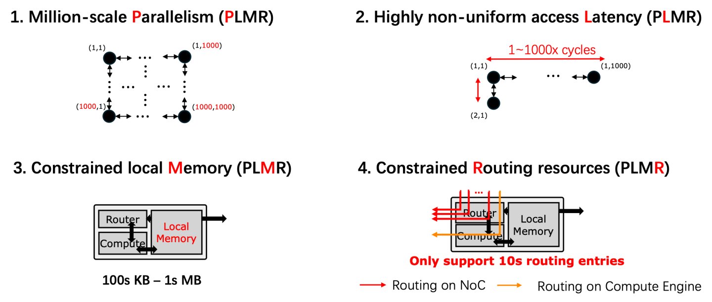
The USENIX piece introduces PLMR, a four-dimensional model for characterizing wafer-scale systems: Parallelism, Locality, Memory capacity, and Routing. Each dimension maps to a property where wafer-scale hardware diverges sharply from what GPU software assumes.
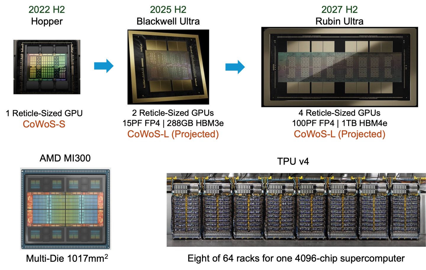
The scale difference is stark. A conventional system-on-die GPU runs at roughly 858 mm2 of area with die-to-die bandwidth in the range of 1 to 10 TB/s and memory bandwidth in the tens of TB/s. A system-on-wafer on the TSMC N3 process node occupies approximately 73,062 mm2, exposes die-to-die bandwidth in the range of 10 to 100+ TB/s, and delivers memory bandwidth in the tens of PB/s, aggregated across its mesh rather than shared through an all-to-all fabric. Energy efficiency of interconnect improves by roughly two orders of magnitude: die-to-die transfers on a conventional chip cost tens of picojoules per bit, while wafer-scale interconnect operates at tenths of picojoules per bit.
The critical difference for software is the memory model. A GPU cluster uses a small number of devices, each holding a large block of contiguous memory accessible to all threads on that device. A wafer-scale chip gives each core a small block of local fast memory and requires explicit routing of data between cores through the mesh interconnect. The programming model is inherently distributed and asynchronous at a fine granularity, rather than the coarser distributed-but-shared model GPU clusters use.
Existing AI compilers were designed for the GPU model. They partition a computation into kernels, map kernels to GPU threads, and rely on the GPU’s hardware memory hierarchy to handle communication within a device. Applying the same approach to a wafer-scale chip means either ignoring the mesh topology and leaving performance on the floor, or retooling every layer of the stack from IR representation through scheduling to runtime communication.
WaferLLM: What the System Level Requires
WaferLLM, the LLM inference system that preceded Wavel and MeshRT as research output from the same research group, demonstrates what correct placement and routing on a wafer-scale mesh actually requires. The system organizes inference around PLMR and separates prefill from decode because the two phases have different memory and computation profiles that call for different mesh strategies.
For prefill, where the input tokens are processed in a single large matrix multiplication, WaferLLM uses MeshGEMM: a matrix multiplication algorithm designed for a 2D core mesh that uses cyclic shifts to move data through the mesh and interleaves communication with computation to prevent cores from stalling while waiting for data to arrive. This is not a conventional GEMM kernel mapped to a mesh; it requires explicit reasoning about mesh topology in the algorithm design.
For decode, where a single new token is generated at a time using a vector-matrix multiply, WaferLLM uses MeshGEMV with a tree-based all-reduce strategy suited to the smaller communication pattern of single-token generation. Independent benchmark summaries report gains of 160 times over the T10 baseline and 625 times over the Ladder baseline, though these numbers come from secondary sources and should be verified against the primary paper before relying on them.
The demonstrated result is sub-millisecond-per-token inference latency. That figure matters because it suggests that wafer-scale integration is not just a path to running larger models; it is a path to running any model faster in ways that matter for interactive applications.
Wavel and MeshRT: The Compiler and Runtime Response
WaferLLM showed what was possible with carefully hand-crafted mesh algorithms. Wavel and MeshRT, both in the SOSP 2026 program, address what the compiler and runtime must look like to make that kind of optimization systematic rather than manual.
Wavel is a compilation system for wafer-scale accelerators. The core challenge a wafer-scale compiler faces that a GPU compiler does not is placement: deciding which layers and operations run on which regions of the mesh, and how activations and weights route between them. A GPU compiler can treat a single device as a uniform memory space. A wafer-scale compiler must reason about the mesh topology when assigning computation, because the cost of routing data between two cores depends on their physical distance.
MeshRT takes a different angle on the same architecture. Where Wavel focuses on the compilation step, MeshRT moves runtime governance decisions into compile time. The premise is that for low-latency, high-throughput inference, the overhead of making scheduling and routing decisions at runtime is too high. By determining at compile time exactly how execution will proceed and baking those decisions into the compiled artifact, MeshRT aims to reduce the runtime decision overhead that would otherwise add latency to every generated token.
Together they describe a two-phase approach that matches how inference systems are deployed in practice: compile once (with Wavel doing topology-aware placement), then run repeatedly (with MeshRT executing a pre-committed schedule rather than dynamically adapting). The pair at SOSP 2026 represents the first peer-reviewed compiler and runtime designed specifically for wafer-scale inference, published in the same venue as LLM-42’s deterministic serving work.
The Commercial Stack: Cerebras and the AMD Partnership
Cerebras is the only company currently shipping wafer-scale hardware at commercial scale. The CS-4 system combines three WSE-3 Turbo processors in a redesigned rack with wafer-scale backpacks that integrate power conversion, liquid cooling, high-speed I/O, and control electronics. Cerebras reports more than 1,000 tokens per second on models exceeding 10 trillion parameters.
The Cerebras software stack provides a concrete production reference for what the research papers are pointing toward. The graph compiler takes a PyTorch model, determines per-core placement, tensor layouts, tiling strategies, kernel generation, and on-wafer communication schedules, then emits a target-specific executable with metadata that the runtime uses. No CUDA kernels, no GPU thread hierarchy: the abstraction is entirely different. Weight streaming via MemoryX allows the on-chip SRAM to hold activations while model weights are streamed from external memory, keeping the 44 GB of on-wafer SRAM dedicated to the active computation.
On July 23, 2026, AMD and Cerebras announced an inference configuration that combines GPUs and a WSE in a single pipeline. GPUs handle parts of the inference workload, and the Cerebras chip handles the rest. This heterogeneous arrangement is practically significant because it acknowledges that neither chip type is optimal for every part of LLM inference, and that the system software problem now includes managing handoffs between radically different memory models at inference time.
Limitations and Open Questions
Both Wavel and MeshRT are research systems presented at SOSP 2026. Neither has a publicly available production codebase as of September 2026. The SOSP artifact pages may include evaluation artifacts, but the full compiler and runtime implementations are not yet available for external teams to adopt. WaferLLM’s benchmark numbers come partly from secondary technical summaries, and the primary paper numbers should be used for any engineering evaluation.
The transition from GPU-era thinking to wafer-scale thinking requires changes at every layer: model architecture design to exploit mesh locality, compiler support for topology-aware placement, runtime protocols for distributed asynchronous execution, and training infrastructure that matches the target inference hardware. Most teams cannot rearchitect all of these layers at once. The near-term practical path for most organizations is through Cerebras’s managed stack, which abstracts the hardware complexity.
Manufacturing defect handling remains a non-trivial engineering concern. Cerebras includes redundant links and cores; when defective regions appear, the hardware driver performs a remapping to preserve a virtually intact 2D mesh topology. Software written against the full mesh may behave differently when a remapped topology is in use, though Cerebras’s driver is designed to hide this from application code.
What This Means for Engineering Teams
The relevant question for teams building on AI infrastructure is not whether wafer-scale hardware is faster. It clearly is, on the metrics that matter for inference. The relevant question is at which layer the investment in wafer-scale specificity pays off, and when.
For most teams today, the answer is: use Cerebras’s managed stack and treat the hardware as a fast inference appliance. The PLMR framework is useful for reasoning about whether a given model’s memory and communication pattern will map well to a mesh, but that reasoning does not require implementing a custom compiler. The research papers from Wavel and MeshRT matter most for teams inside companies building wafer-scale hardware or compilers, and for teams at the frontier of inference-latency requirements who are willing to invest in low-level systems work.
What the SOSP 2026 papers collectively signal is that wafer-scale inference is developing its own systems research stack, not just specialized silicon. That is a stronger signal than hardware performance numbers alone: it means the software tooling necessary to program these machines systematically is now being built and evaluated by independent research groups, not just by chip vendors. For teams building on large-scale AI models, that trajectory is worth tracking even if wafer-scale hardware is not in the near-term procurement plan.
Key Takeaways
- Wafer-scale chips (e.g., Cerebras WSE-3: 900,000 cores, 44 GB on-wafer SRAM, 21 PB/s memory bandwidth) expose a mesh architecture that invalidates GPU-era compiler and runtime assumptions.
- Congjie He et al.’s PLMR framework (Parallelism, Locality, Memory capacity, Routing) articulates the four dimensions where wafer-scale hardware differs from conventional systems-on-die.
- WaferLLM demonstrates sub-millisecond-per-token latency using MeshGEMM (cyclic-shift-based matrix multiplication for prefill) and MeshGEMV (tree-based all-reduce for decode).
- Wavel (topology-aware compilation) and MeshRT (compile-time-governed runtime), both at SOSP 2026, provide the first peer-reviewed compiler and runtime designed specifically for wafer-scale AI inference.
- The AMD and Cerebras July 2026 partnership combines GPUs and wafer-scale processors in one inference pipeline, showing that heterogeneous serving is the practical near-term path.
- Research system status: Wavel and MeshRT are academic publications, not yet public production systems; Cerebras’s commercial stack is the current practical option.
Work With Origins AI
Origins AI builds production AI systems for engineering teams. If your inference architecture is hitting throughput or latency limits that GPU clusters cannot solve, talk to our team.